- 您现在的位置:买卖IC网 > Sheet目录1992 > CY28317PVXC-2 (Silicon Laboratories Inc)IC CLK FTG VIA PL/E133T 48SSOP
CY28317-2
..................... Document #: 38-07094 Rev. *B Page 19 of 20
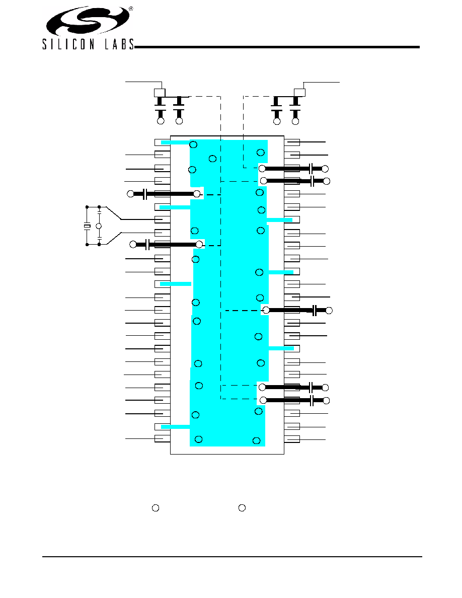
Layout Diagram
G = VIA to GND plane layer
V = VIA to respective supply plane layer
Note: Each supply plane or strip should have a ferrite bead and capacitors
G
FB
+3.3V Supply
C4
Ceramic Caps C3 = 10–22 F C4 = 0.005 F
10
F
FB = Dale ILB1206 - 300 (300
@ 100 MHz) or TDK ACB2012L-120
0.005
F
G
VDDQ3
C3
C6 = 0.01
F
48
47
46
45
44
43
42
41
40
38
37
36
35
34
33
32
31
30
29
28
27
26
25
1
2
3
4
5
6
7
8
9
10
11
12
13
14
15
16
17
18
19
20
21
22
23
24
39
G
V
CY28317-2
G
V
G
V
G
V
G
V
G
FB
+2.5V Supply
C4
10
F
0.005
F
G
VDDQ2
C3
G
V
G
V
G
发布紧急采购,3分钟左右您将得到回复。
相关PDF资料
CY28323OXC
IC CLOCK BROOKDALE GPENT4 48SSOP
CY28354OXC-400
IC BUFF 273MHZ 4DDR DIMM 48SSOP
CY28378OXC
IC CLOCK CK408/TITAN 845 48SSOP
CY284108ZXC
IC CLOCK SERV CK410B 56TSSOP
CY28410OXC-2
IC CLOCK CK410 GRANTSDALE 56SSOP
CY28410OXC
IC CLOCK CK410 GRANTSDALE 56SSOP
CY28411ZXC
IC CLOCK CK410M ALVISO 56TSSOP
CY28442ZXC-2
IC CLOCK ALVISO PENTM 56TSSOP
相关代理商/技术参数
CY28317PVXC-2T
功能描述:时钟发生器及支持产品 NB Clk VIA SDRAM Chipsets / Tualatin RoHS:否 制造商:Silicon Labs 类型:Clock Generators 最大输入频率:14.318 MHz 最大输出频率:166 MHz 输出端数量:16 占空比 - 最大:55 % 工作电源电压:3.3 V 工作电源电流:1 mA 最大工作温度:+ 85 C 安装风格:SMD/SMT 封装 / 箱体:QFN-56
CY28317ZC-2
制造商:CYPRESS 制造商全称:Cypress Semiconductor 功能描述:FTG for Mobile VIA PL133T and PLE133T Chipsets
CY28317ZC-2T
制造商:CYPRESS 制造商全称:Cypress Semiconductor 功能描述:FTG for Mobile VIA PL133T and PLE133T Chipsets
CY28322
制造商:未知厂家 制造商全称:未知厂家 功能描述:Clocks and Buffers
CY28322-2
制造商:CYPRESS 制造商全称:Cypress Semiconductor 功能描述:133-MHz Spread Spectrum Clock Synthesizer with Differential CPU Outputs
CY28322ZC-2
制造商:Rochester Electronics LLC 功能描述:- Bulk
CY28322ZC-2T
制造商:Rochester Electronics LLC 功能描述:- Bulk
CY28323
制造商:CYPRESS 制造商全称:Cypress Semiconductor 功能描述:FTG for Intel㈢ Pentium㈢ 4 CPU and Chipsets